

Silicon wafers are the fundamental building blocks of modern electronics. They are used in everything from computer processors and memory chips to photovoltaic cells in solar panels. Silicon, a semiconductor material, is chosen because of its electrical properties, making it ideal for fabricating integrated circuits and other electronic components. However, the process of making silicon wafers is highly complex, involving multiple stages of purification, crystallization, and shaping.
In this article, we’ll explore the process of making silicon wafers from raw materials to the final product, ready for use in semiconductor manufacturing.
1. Raw Material Extraction: Obtaining Silicon
The process begins with the extraction of silicon from its natural form. Silicon is the second most abundant element in the Earth’s crust, and it is most commonly found in the form of silica (SiO₂), usually as quartz or sand.
- Silicon mining: Silica is mined from natural sources such as sand or quartzite rock. It is then transported to a facility where it undergoes a purification process.
2. Purification: Refining Silicon
The silicon used in electronic applications must be extremely pure, with impurities reduced to levels of less than one part per billion. This level of purity is necessary to ensure the silicon’s optimal electrical conductivity. The purification process includes the following steps:
a. Reduction of Silica to Metallurgical-Grade Silicon (MG-Si)
The first step is to reduce silica into silicon metal through a chemical reduction process:
- Silica (SiO₂) is mixed with carbon and heated in an electric arc furnace to temperatures over 2,000°C.
- This results in the following chemical reaction: SiO₂ + C → Si + CO₂.
- The output is metallurgical-grade silicon (MG-Si), which is approximately 98% pure.
b. Converting MG-Si to Electronic-Grade Silicon (EG-Si)
To achieve the required level of purity for semiconductor applications, the MG-Si is further refined into electronic-grade silicon (EG-Si):
- Chemical purification: The silicon is reacted with hydrogen chloride (HCl) at high temperatures to form trichlorosilane (SiHCl₃), a volatile compound.
- Fractional distillation: The trichlorosilane is purified through fractional distillation, which separates impurities from the silicon compound.
- Decomposition: The purified trichlorosilane is decomposed at high temperatures in a chemical vapor deposition (CVD) reactor to yield pure silicon.
At the end of this process, the result is polycrystalline silicon (polysilicon) with a purity level of 99.9999% or higher.
3. Crystal Growth: Creating a Silicon Ingot
The next step is to transform the purified polysilicon into a single crystal silicon structure, known as a silicon ingot. The most common method for growing a single crystal ingot is the Czochralski (CZ) process, though there is also an alternative process called Float Zone (FZ).
a. Czochralski (CZ) Process
The CZ process involves melting high-purity polysilicon in a crucible, typically made of quartz, at a temperature of around 1,425°C. A small, seed crystal of silicon, which has the desired crystalline orientation, is dipped into the molten silicon. The seed crystal is slowly withdrawn while being rotated, allowing the silicon atoms to solidify around the seed in a continuous single crystal structure.
- Ingot formation: The seed crystal is pulled upward very slowly, causing the molten silicon to solidify around it and form a cylindrical silicon ingot, often 1-2 meters long and up to 300mm (12 inches) in diameter.
- Crystal orientation: The crystal orientation of the ingot is crucial for the electronic properties of the final wafer and is maintained by carefully controlling the conditions of the CZ process.
b. Float Zone (FZ) Process (Alternative)
In the FZ process, a high-purity polysilicon rod is melted using a localized heating source, and the molten zone is passed along the rod to purify and crystallize the silicon. This process avoids contamination from a crucible and produces highly pure silicon, although it is typically used for specialized applications.
4. Cutting: Slicing the Ingot into Wafers
Once the silicon ingot is formed, the next step is to slice it into thin wafers. This process involves the following:
- Orientation and grinding: The ingot are first shaped into a perfect cylindrical form by grinding the outer surface. It is then carefully aligned to ensure the proper orientation of the crystal structure.
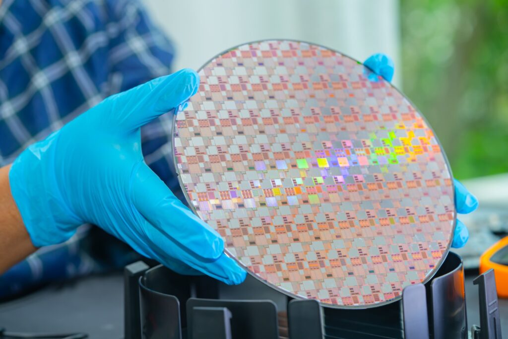
- Slicing the ingot: The ingot is sliced into thin wafers using a diamond wire saw. The thickness of the wafers typically ranges from 100 to 200 microns. These thin wafers will serve as the base material for semiconductor device fabrication.
- Flat or notch: A flat or notch is often added to the wafer to indicate the crystal orientation and type of doping (p-type or n-type).
5. Lapping and Polishing: Surface Preparation
After slicing, the wafers have rough surfaces due to the cutting process, so they must be smoothed through lapping and polishing to make them suitable for semiconductor manufacturing.
- Lapping: The wafers are initially lapped to remove saw marks and create a flatter surface. This process involves rubbing the wafer between two hard surfaces with an abrasive slurry, which helps reduce the thickness variation across the wafer.
- Polishing: After lapping, the wafers undergo chemical-mechanical polishing (CMP) to achieve a mirror-like, smooth surface. The polished wafers are extremely flat, with surface variations measured in nanometres. This precision is essential for subsequent semiconductor fabrication processes, where even the slightest imperfection can affect the performance of microchips.
6. Doping: Adding Electrical Properties
In many cases, silicon wafers need to be doped to modify their electrical properties. Doping involves introducing small amounts of impurity atoms, such as boron (p-type doping) or phosphorus (n-type doping), to create the necessary electrical characteristics for semiconductor devices. Doping can be done through high-temperature diffusion or ion implantation, where ions of the desired element are implanted into the silicon crystal.
7. Cleaning and Inspection: Ensuring Quality
After polishing and doping, the wafers are thoroughly cleaned to remove any remaining particles, organic residues, or metal contaminants. This is typically done in a series of chemical baths using highly purified water and cleaning agents like hydrofluoric acid (HF).
Following cleaning, the wafers undergo strict inspection using various metrology tools to ensure they meet the necessary specifications in terms of thickness, flatness, and cleanliness. Wafer defects are identified and removed, and only wafers that meet quality standards are sent forward for semiconductor fabrication.
8. Final Steps: Wafer Marking and Packaging
Before the wafers are shipped to semiconductor manufacturing facilities, they undergo final processing steps, including:
- Wafer marking: Each wafer is etched with a unique identifier or barcode using a laser, allowing manufacturers to track it through the fabrication process.
- Packaging: The wafers are placed in wafer carriers or cassettes to prevent contamination and damage during transport.
The process of making silicon wafers is highly intricate, requiring precise control over multiple steps to ensure the highest levels of purity and crystal perfection. From the raw material of silicon dioxide to the final wafer, ready for semiconductor fabrication, every stage is critical in producing wafers that meet the stringent demands of the electronics industry.
By the time the wafers reach the semiconductor fabrication facility, they have undergone a lengthy journey through chemical reactions, crystallization, cutting, polishing, and inspection. These wafers will soon become the foundation for the integrated circuits and chips that power our modern world, from smartphones and computers to cars and renewable energy technologies.